Premier Pilot Plant People
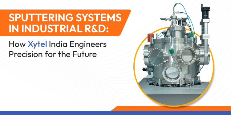
Sputtering Systems in Industrial R&D: How Xytel India Engineers Precision for the Future
Sputtering Systems in Industrial R&D: How Xytel India Engineers Precision for the Future
Meeting the Demands of Modern Materials Science
In today’s advanced manufacturing landscape, the need for precise, reliable, and scalable thin film deposition systems is more critical than ever. Whether for semiconductors, optics, or high-performance coatings, sputtering systems have emerged as an indispensable tool for R&D facilities and pilot-scale plants. At the heart of this technology is the physical vapor deposition (PVD) process — a technique that relies on controlled plasma environments to deposit ultra-thin layers of metal or dielectric materials onto a target substrate. But designing a sputtering system that meets stringent research demands while offering flexibility, scalability, and engineering robustness is no small feat. This is where Xytel India steps in — offering custom-built sputtering systems engineered for excellence in industrial research and development environments.What Is Sputtering and Why Does It Matter
Sputtering is a physical vapor deposition method where atoms are ejected from a solid target material due to bombardment by energetic plasma ions. These atoms then condense onto a substrate, forming a thin, uniform film. It’s a process favored for its:- High film adhesion and density
- Uniform thickness control
- Scalability for multiple material types
- Clean deposition environment
- Semiconductors: Thin layers of conductive or insulating materials
- Optical coatings: Anti-reflective or scratch-resistant films
- Surface engineering: Protective or functional coatings for tools and components
- Energy research: Solar cell material deposition
- Aerospace and defense: Precision coatings for sensitive equipment
Common Challenges in Sputtering System Design
Despite its advantages, sputtering systems come with complex engineering challenges:- Maintaining stable vacuum conditions
- Achieving uniform film thickness over various substrate sizes
- Managing plasma power inputs (DC, RF, or pulsed)
- Incorporating in-situ diagnostics for real-time monitoring
- Handling temperature-sensitive substrates
- Offering flexibility for multi-material or multi-layer deposition
Xytel India’s Approach: Engineering Custom Sputtering Systems That Work
At Xytel India, we understand that pilot-scale sputtering systems must be flexible, precise, and robust. Every system we design is tailored to your specific research needs — whether you’re evaluating new materials, scaling up processes, or running continuous tests for product development.Key Features of Xytel India’s Sputtering Systems:
- Precision Vacuum Control
- High-integrity vacuum chambers to ensure minimal contamination and consistent deposition quality.
- Advanced Plasma Source Integration
- Systems are built to support DC, RF, or pulsed plasma power supplies, depending on the application.
- Stable plasma environments for repeatable thin film characteristics.
- Custom Substrate Handling Mechanisms
- Fixed, rotary, or planetary substrate holders for optimal uniformity.
- Substrate temperature control for sensitive deposition requirements.
- Multi-Material and Layer Support
- Multi-target configurations enabling sequential or co-sputtering for layered film structures.
- In-Situ Monitoring and Diagnostics
- Real-time sensors and monitoring tools to fine-tune deposition parameters.
- Integrated control systems to adjust film thickness and rate dynamically.
- Material Versatility
- Designed to handle a wide range of metals, oxides, nitrides, and dielectrics — suitable for research in evolving materials.
Built for Pilot Plants and Industrial R&D
Unlike commercial off-the-shelf units, Xytel India’s sputtering systems are built to serve pilot plants, material science labs, and industrial R&D environments. Our systems are engineered for:- Rapid prototyping and experimentation
- Process parameter optimization
- Scalability assessment before mass production
- Integration with existing plant control systems
Designed for Your Industry
Xytel India’s systems are currently suited to — and customizable for — the following sectors:- Semiconductor R&D
- Energy technology (photovoltaics, fuel cells)
- Aerospace and defense coatings
- Medical device surface engineering
- Optoelectronics and display technology
Why Choose Xytel India?
For over 40 years, Xytel has been known for designing and fabricating high-performance pilot plants and process systems. Our sputtering systems embody the same spirit: engineered with precision, built for flexibility, and designed to serve the most demanding research environments. When you work with Xytel India, you gain:- End-to-end collaboration from concept to commissioning
- Custom mechanical and electrical design
- Integration with your existing automation or control infrastructure
- Long-term support and optimization services
Conclusion: Let’s Engineer the Future of Thin Film Deposition
Sputtering systems are foundational to modern innovation, but to unlock their full potential, you need systems that reflect the specific needs of your research or industrial application. Xytel India offers more than just equipment — we offer engineering solutions that adapt to your goals and accelerate your progress.Ready to design your next sputtering system?
Let’s start a conversation about your pilot-scale or R&D sputtering needs. Our engineers are ready to work with you, from the drawing board to deployment. 👉 Contact Xytel India TodayGet in Touch
You will be amazed as how partnering with us becomes a game changer in your quest for R&D glory.