Premier Pilot Plant People
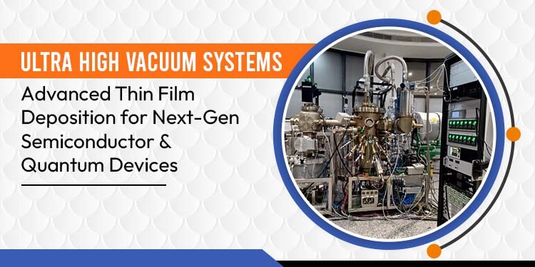
Ultra High Vacuum Systems: Advanced Thin Film Deposition for Next-Gen Semiconductor & Quantum Devices
Ultra High Vacuum Systems: Advanced Thin Film Deposition for Next-Gen Semiconductor & Quantum Devices
The rapid progress of semiconductors, quantum devices, and photonics is driven by one crucial capability, the ability to grow thin films with atomic precision. Achieving this requires Ultra High Vacuum (UHV) systems, where deposition environments are controlled to the highest standards of purity and accuracy. Today, UHV platforms are at the heart of research in next-generation electronics, quantum computing, optoelectronics, and 2D materials. Let’s explore how advanced deposition solutions are shaping the future and how companies like Xytel India, in collaboration with Vinci Technologies, are bringing these systems to researchers and industries across India.Why Ultra High Vacuum Systems Matter
Thin films are the building blocks of modern devices. Whether it’s semiconductor heterostructures, gallium nitride (GaN)-based electronics, or two-dimensional transition metal dichalcogenides (TMDCs), precise deposition under ultra-clean conditions ensures high performance and reliability. UHV systems provide:- Contamination-free environments for growth.
- Atomic-level thickness control for reproducible films.
- Flexibility across materials — metals, oxides, and 2D materials.
Our UHV Platforms
Different applications demand different deposition technologies. The UHV platforms available today cover a wide spectrum:- Thermal & E-beam Evaporator – Reliable metal deposition.
- Magnetron Sputtering System – DC & RF sputtering systems for metals and metal oxides.
- Molecular Beam Epitaxy (MBE) – Includes 2D-MBE systems for TMDCs growth and dedicated GaN MBE systems.
- Pulsed Laser Deposition (PLD) – 8-target PLD systems for versatile film growth.
- Hybrid Systems – Combining MBE, E-beam, Thermal, and Sputtering for a wide range of materials, including 2D-TMDCs and complex oxides.
System Specifications
Each platform is designed with research precision in mind:- Thermal & E-beam Evaporator – Delivers consistent and reliable thin metal films.
- Magnetron Sputtering – Available in both DC & RF configurations; suitable for robust deposition of metals and oxides.
- Molecular Beam Epitaxy (MBE) – Tailored systems for 2D materials and GaN-based devices.
- Pulsed Laser Deposition (PLD) – Equipped with an 8-target system to handle diverse materials.
- Hybrid Configurations – Ideal for multi-material research needs, bridging different deposition techniques under one UHV chamber.
What We Provide
UHV systems are not off-the-shelf tools. They require careful customization, integration, and support. Here’s what Xytel India and Vinci Technologies provide to researchers and industry partners:- Customized systems designed around specific research needs.
- Scalable integration for semiconductor, photonics, and quantum research facilities.
- Versatility for depositing a broad range of materials.
- Advanced control features for precise process repeatability.
- Compact and accurate designs for optimized lab usage.
- Local support in India, including installation, commissioning, application, and maintenance.
- Process demonstrations based on real-world research applications.
Our Systems in India
Cutting-edge UHV systems are already operational across premier research institutions. 2D-MBE and Sputtering systems are in use across IITs and centrally funded research institutes, enabling Indian researchers to advance semiconductor and quantum device development domestically.Bridging the Gap: The Issue
While Xytel India has an established global footprint in pilot plants, modular engineering, and automation systems, their entry into the semiconductor and quantum domains highlights a key challenge: the need for clear, specialized communication around UHV thin film deposition systems. The technology demands more than engineering excellence; it requires proof of ultra-clean vacuum levels, precision in thin-film growth, and application-driven results. By aligning technical specifications with case studies, success stories, and detailed performance data, Xytel can strengthen its position as a credible partner for India’s semiconductor and quantum ecosystem.Conclusion
As India pushes forward in semiconductor manufacturing, quantum research, and advanced materials, UHV thin film deposition systems will play a defining role. With platforms such as MBE, PLD, sputtering, and hybrid systems, researchers are equipped to fabricate next-generation devices with unmatched precision. By combining global expertise with local support, customization, and advanced control systems, Xytel India and Vinci Technologies are enabling researchers to bridge the gap between ideas and scalable quantum-ready technologies.Get in Touch
You will be amazed as how partnering with us becomes a game changer in your quest for R&D glory.